Reading Assignments and Exercises
This course is designed to provide you with basic concepts and techniques that will get you started in understanding and analysis of hardware and software interaction in computer systems. Computing is a rapidly changing field, with processor speed doubling every 1.5 years, and entire computer systems becoming obsolete in two to four years. In this course, you will learn how computers work, how to analyze computer performance, and what issues affect the design and function of modern computers.
The development of computers since the late 1930s has led to the corresponding development of a variety of software and hardware tools and capabilities. In this section of our course notes, we review several key concepts that you are likely to encounter in this course, and in practice. In particular, this section reviews the use of abstractions, technology, logic design, and performance assessment. This section is organized as follows:
- 1.1. Introduction and Overview
1.2. Overview of Computer Abstractions
1.3. Overview of Computer Technology Trends
1.4. Digital Logic Design
1.5. Computer Performance Assessment
1.6. Performance Benchmarking
Information contained herein was compiled from a variety of text- and Web-based sources, is intended as a teaching aid only (to be used in conjunction with the required text, and is not to be used for any commercial purpose. Particular thanks is given to Dr. Enrique Mafla for his permission to use selected illustrations from his course notes in these Web pages.
1.1. Introduction and Overview
Reading Assignments and Exercises
Computers are comprised of software and hardware. In previous programming classes, we studied how high-level software could be used to drive computer hardware. In this course, we concentrate on the development of hardware, and show how it supports the execution of software at a low level.
1.1.1. Course Overview and Objectives
This course is designed to convey some "big ideas" about computing, with enough low-level support and knowledge to understand the practical uses and implications of these ideas, which are:
Five components of a computer - memory, datapath, control, input, and output, which are used in modern digital computing machines.
Data can be anything - integers, floating point, characters, bitstream. The actual values and use of data are determined by the program (software) running on the computer.
Stored program - instructions in memory can be thought of as data. They can be accessed randomly or sequentially, and can be input or output (read or written in and out, respectively) to increase memory utilization.
Principle of locality - in a given (small) time slice, most memory I/O is done in a small cluster of addresses. The phenomenon of locality supports scheduling and prediction of memory accesses, which enables devices like caches to work efficiently.
Parallelism - many processors can work together efficiently to solve a problem, which increases performance and decreases execution time.
Composition - allows us to build complex systems by first starting with small components, then building larger components from the smaller ones.
Abstraction - supports the naming and description of complex, low-level system objects with high-level constructs that are more easily understood by humans.
Compilation versus Interpretation - a key issue when considering computer language implementation and use. Compilation uses software to directly produce executable code that can be optimized to run on a given machine. Interpretation attempts to execute source code by translating it into executable code just prior to execution. Because optimizations are hard to perform dynamically, reduced system performance tends to result.
Principles and Pitfalls of Performance Measurement - know what you are measuring, where and how to measure it, when a given measurement (or metric) is useful, and why a given metric works (or doesn't work) in a given situation.
1.1.2. Course Overview and Objectives
In order to convey this information, we have a highly detailed textbook, from which the following topics will be drawn:Abstraction and Technology - Chapter 1
Performance Measurement - Chapter 2
Instruction Set Architecture - Chapter 3
Arithmetic and ALU Design - Chapter 4
CPU Design and Execution - Chapter 5
Pipelining for Increased Performance - Chapter 6
Memory: Cache, Main, Virtual - Chapter 7
I/O Devices and Protocols - Chapter 8
1.1.3. Origins and History
In this section, we present a brief overview of computer history. Additional information can be found at The Digital Century link.
In this historical epoch, computers were first developed by the Egyptians, who had the abacus and shadow clocks. In the pre-industrial era, mechanical calculators were developed by Pascal and Leibniz. During the Industrial Revolution, mechanical computers were envisioned, and parts of such machines were prototyped, by Charles Babbage. These computers were not constructed in their entirety, due to size, weight, and power requirements that could not be satisfied by the technology of the day. An interesting overview of early mechanical computers is given in this link.
With the discovery of electricity, electronic tabulating machines were developed by Herman Hollerith, whose company was purchased by Thomas Watson, founder of the International Business Machines Corporation. Throughout the 1920s and 1930s, IBM marketed a variety of tabulating machines driven by electrified keyboards and having a variety of printers. Although unsophisticated, this type of hardware helped the business community become accustomed to the idea of machine-assisted inventory, payroll, and shipping. Additionally, the hardware developed by IBM was modified for use in its early computers. Thus, it could be said that the era of electro-mechanical tabulating machines in some ways prepared society for the advent of digital computers.
The advent of World War II increased the demand for more accurate calculations. Rooms full of humans were employed in computing artillery trajectories, and the result was unacceptable error. A variety of computing research projects were undertaken at Princeton University, Harvard University, and the University of Pennsylvania. These resulted in room-size computers such as the Mark-I through Mark-IV, and the ENIAC, all of which used vacuum tubes. The vacuum tube machines were erroneous (tubes burned out or their response drifted frequently), power-intensive, slow (less than 10,000 integer multiplications per second), and hard to program, but provided a useful testbed for basic computer concepts.
After WWII, the business community was slow to accept computers because of their cost, size, weight, power consumption, and the cost of maintaining them (including programmer salaries). However, the Defense Department funded computer research during the early years of the Cold War, from which resulted the second generation of computers. These machines used transistors instead of vacuum tubes, and were smaller, less power-consumptive, and easier to use. Business firms became more interested in computing, and IBM started to manufacture business and scientific computers (4000 and 7000 series, respectively).
In the 1960s, transistors were integrated first on small circuit boards, then etched on wafers called integrated circuits. These were much smaller than the second-generation computer circuits, and predictably consumed less power, took up less space, and were easier to repair (or replace). In the 1960s, many electronics companies were in business that are no longer building digital computers today - General Electric, RCA, Honeywell, and Burroughs, to name but a few. IBM's System/360 was the first general-purpose computer to support both business and scientific calculations, and had a number of operating system features that were novel for its day, including upward compatibility of software, programmability of the operating system through a (dreadful) language called OS/JCL, as well as support for numerous programming languages.
The 1970s saw the advent of much faster and more capable integrated circuits, which made computers smaller and faster. IBM's System/370 was the workhorse mainframe series of the era, but was challenged by similar architectures, such as those produced by the Ahmdahl Corporation. In the 1970s, two important trends developed in addition to mainframe computing. First, the supercomputer was developed largely due to the efforts of Seymour Cray, who pioneered high-performance computing in the 1960s with the CDC6600 that he developed for Control Data Corporation. Second, the minicomputer was developed by Digital Equipment Corporation (DEC), whose PDP series of machines was the first general-purpose computer that small universities or research laboratories could afford. A third trend that went almost unnoticed, was the gradual emergence of personal computers, which were initially the domain of hobbyists. From these early beginnings came the Apple-II, the world's first affordable, workable personal computer that could be operated in some ways like its larger ancestors (mainframe or the minicomputer).
In the 1980s, integrated circuits gave way to very large scale integrated (VLSI) circuit technology, which eventually packed millions of transistors onto a single chip. This comprised the fourth generation of computing machine technology. As a result, personal computers became smaller and faster, posing a challenge to the minicomputer. The use of VLSI technology enabled companies like DEC to compete with the mainframe market by developing superminicomputers. On the personal computer side of the market, IBM introduced the IBM/PC in 1980, which revolutionized the desktop by providing a common, open architecture. A young fellow, who combined ideas from DEC's VMS operating system and the emerging UNIX operating system, headed a company that was chosen to write the first extensible PC operating system - MS-DOS. The rest, as they say, is history - Bill Gates and Microsoft rose with IBM and its processor developer Intel to become the dominant players in a multi-billion-dollar industry, which eventually eclipsed the mainframe market and consigned minicomputers, superminicomputers, and microcomputers to the dustbin of history (for all but the most highly customized applications).
The 1990s saw the emergence of distributed or networked computing and the continued proliferation of personal computers. Another development of the 1990s was mobile computing, which could become the dominant paradigm for personal computing in the first decade of the new millenium. On the supercomputer front, massively parallel machines were developed to become more practical, easier to program, and small enough for a mid-sized university to purchase for research or teaching purposes. Parallel computer technology continues to grow, supported in part by ever-smaller integrated circuit components and more user-friendly software. Distributed technology continues to proliferate both in computing and communication. The Internet and World-Wide Web have unified these paradigms to become the dominant platforms for the computerized dissemination of knowledge.
If you would like to read more, check out the Hitmill History of Computers Website. For a comprehensive trip through computer history, visit the Computer History Museum.
1.2. Overview of Computer Abstractions
Reading Assignments and Exercises
As shown in Figure 1.1, computer systems span many levels of detail, which in computer science we call levels of abstraction. This hierarchy is reviewed in Appendix B.
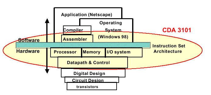
Figure 1.1. Levels of abstraction in computer systems,
adapted from [Maf01]
In this course, we are concerned with the following components:
Operating System - Provides a convenient interface between (a) the user and his/her application software, and (b) the hardware (sometimes called the bare machine).
Assembler - Translates assembly language, a primitive type of programming language, into machine code, which is a stream of ones and zeroes.
Instruction Set Architecture(ISA) - Interfaces the software (listed above) to the hardware (listed below), and provides support for programming.
Processor, Memory, and I/O System - These components support the execution of machine code instructions expressed in terms of the ISA.
Datapath and Control - Provide a convenient abstraction for connecting the processor, memory, and I/O system and controlling their function efficiently.
If you have taken Dr. Mafla's version of this course, you will be acquainted with the following five components of a computer:
- Input - Provides data and program information
- Datapath - Mediates I/O
- Control - Implements control of calculation and communication or I/O processes
- Memory - Storage and retrieval of programs or data
- Output - Result of running program on processor using input
1.2. Overview of Computer Abstractions
Reading Assignments and Exercises
Abstractions help us express intangible concepts in visible representations that can be manipulated. For example, a data structure is an abstraction that organizes concepts or numbers in a comprehensible, organized representation that can be manipulated by a computer program. Figure 1.2 illustrates another view of a computer system, which is comprised of different levels of language and means of translating these languages into lower-level languages. Finally, the microprogram is loaded onto the hardware.
1.2.1. Different Abstract Views
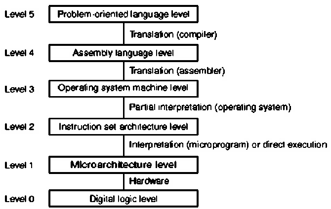
Figure 1.2. Another view of levels of abstraction in computer systems,
adapted from [Maf01].
The salient concepts for Figure 1.2 are listed as follows:
Level 5 - Problem Oriented Language - Provides a convenient interface and applications engine that helps the user produce results specific to a given application area. For example, Microsoft Word is used for document creation or editing, Excel for accounting spreadsheets, etc. The language at this level is usually a sequence of keystrokes or a high-level scripting language. In software design, the language is a high-level programming language such as C, C++, or Java.
Level 4 - Assembly Language - Assembly is a very detailed language that helps the systems programmer or software designer move information around in a computer architecture in a highly specific way. For example, many compilers (programs that translate programming language into an assembly-like language) are written in assembly language. The advantage to assembly language is speed and power in accessing various features of the hardware.
Level 3 - Operating System Machine - Provides a convenient interface between assembly language and the abstraction of the hardware architecture's instruction set. Operating systems generally contain many libraries that help a software developer or programmer connect to lower-level system functions (e.g., I/O, memory allocation, etc.) in an organized way.
Level 2 - Instruction Set Architecture (ISA) - One of the most important parts of a computer is the interface between the lowest-level software and the hardware. The ISA includes anything programmers use to make a binary machine language program work correctly, including instructions, I/O, etc. The ISA facilitates design of functionality independent of the hardware.
Level 1 - Microarchitectural Level - Microinstructions are low-level control instructions that define the set of datapath control signals which apply to a given state of a computing machine. The microinstructions, together with their sequencing, comprise the microarchitecture, whose purpose is to rigorously and consistently express the control of logic circuits that comprise the computer hardware. Designing this control in terms of a program that implements machine instructions in terms of simpler microinstructions is called microprogramming.
Level 0 - Digital Logic - The circuitry that makes a digital computer run is called logic. All processes of a digital computer are expressed in terms of functions of ones and zeros, for example, and, or, and not functions. We will review these logic functions in Section 1.4.
A more general view of the abstractions shown in Figure 1.2 is given in Figure 1.3. Note the recursive levels of translation, from an actual machine (digital logic level in Figure 1.2) to various virtual machines (higher levels of abstraction).
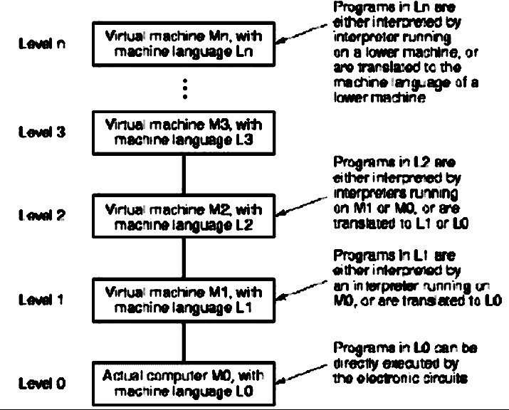
Figure 1.3. Generalized view of levels of abstraction in
computer systems, adapted from [Maf01].
This leads to the following implementational view, where the scope of this course is circled in red.
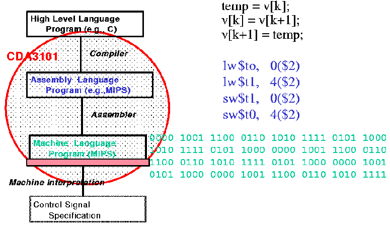
Figure 1.4. Another view of levels of abstraction in computer systems,
adapted from [Maf01].
1.2.2. RISC versus CISC
When computers were first developed, they had very small instruction sets, because the algorithms and hardware for complicated tasks had not yet been developed. As computer design continued into the 1960s, high-level languages (e.g., FORTRAN, Cobol, Lisp) evolved. Hardware designers formed the idea that it might be useful to develop different computers for each type of language - a FORTRAN machine, a COBOL machine, etc. When this approach was tried, it resulted in very complicated instruction sets. Parallel to this development was the IBM philosophy of upward compatibility, which they also tried to implement in hardware. This produced a huge collection of instructions to support all their old computer programs (called legacy code). The result of this was called Complex Instruction Set Computing (CISC), whose philosophy is summarized as follows:
- Bigger is better!
- Make the hardware as "smart" (and, hence, as complex) as possible.
- If you have a great sprawling architecture, that's ok. The hardware fabricators will figure out what to do with your design.
- Don't worry about whether or not the system design is neatly partitioned into layers. (One great sea of logic gates would be ok until we figure out something else that works.)
- When one little part fails, the whole system dies and we will never find out why. That's ok - just build another CPU chip from the ground up. Maybe that one will work better.
CISC has many problems. Some of the bigger problems include lack of maintainability, lack of verifiability, and brittleness. In practice, humans don't know how to verify or maintain really complicated designs. And, we don't yet have software that can perform all the verification and maintenance tasks for us. As a result, as CISC machines got more and more complex, they failed considerably more frequently. This yielded brittle (non-robust) performance in practical computing problems. As the world became more dependent on computers, the CISC design philosophy gradually became unacceptable.
In response to this problem, computer designers returned back to the primitive roots of computer science, and developed the Reduced Instruction Set Computing (RISC) philosophy. The main concept in RISC is that of a very simple Instruction Set Architecture. There is a compact microinstruction set, into which every high-level command or instruction is translated by the compiler. RISC computers tend to run faster, are smaller, and have fewer problems because they have a simple instruction set. The RISC philosophy includes the following concepts:
- Small is beautiful.
- Keep the hardware simple and stupid (KISS design philosophy).
- Hardware and software designers should work together to make the architecture simple and modular.
- Neatly partition the system design into layers, as shown in Figures 1.2 and 1.3. Then, take the vast majority of the functionality that CISC implements in hardware, and put it into software (using compiler transformations) instead.
- Make the hardware and compiler robust, so the entire system can perform reliably.
By keeping the hardware small and modular, the design and fabrication, maintenance, and debugging costs are reduced. This makes sense from an economic perspective. It is also easier to make new generations of RISC computer chips, and to produce them more quickly. This implies potentially greater profits by shortening both the development and product life cycles.
Modularity and simplicity in hardware and software help designers and engineers achieve greater robustness, because the system can be maintained and understood more easily. With simple hardware and software, the functionality of the design can be verified more extensively using software-based testing and proof-of-correctness. Finally, it makes sense to put the CISC complexity into the compiler software, because the software can be modified and corrected much more easily, inexpensively, and quickly than hardware can be changed or updated. Again, this makes good economic sense, because development and re-work costs are significantly reduced.
1.2.3. Concept Summary
Thus far, we have seen that computer hardware (software) evolved in the following stepwise fashion:
Step 1. - Bare logic circuits (plugboard based programming)
Step 2. - Microarchitectural control (machine language programming)
Step 3. - Operating system (batch -> multiprogramming -> time-sharing -> parallelism)
Step 4. - Complex architectures (compilers for high-level languages, e.g., FORTRAN, COBOL -> Pascal -> C -> C++ -> Java)
Step 5. - Hardware/Software interface development (ISA -> CISC -> RISC)
1.3. Overview of Computer Technology Trends
Reading Assignments and Exercises
In Section 1.1, we briefly summarized how technology developed from vacuum tube circuits to modern VLSI techniques. The ability to place more logic gates per unit area has been the primary motivation for exponentially increasing memory and processor capacity and performance. This development has followed several important trends, which we discuss in this section, as follows.
1.3.1. Memory Capacity
Memory capacity has approximately doubled every 1.5 years since the early 1970s. Prior to that, memory was not implemented in integrated circuits, but consisted of arrays of tiny magnetic cores strung together on a lattice of fine wires. Thus, the origin of the term core to describe a computer's main memory. Figure 1.5 illustrates the memory capacity trend, showing how memory gate density has increased from 1 mbegabit (Mbit) per chip in 1986 to 256 Mbit per chip in 2000. By 2004, this is expected to reach 1 Gbit per chip.
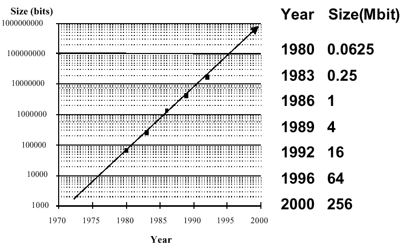
Figure 1.5. Exponential increase in memory capacity as
a function of time since the early 1970s,
adapted from [Maf01].
The increase in memory capacity and processor performance (Section 1.3.3) has made it possible to migrate supercomputer applications such as sophisticated image enhancement, finite-element modelling, and weather prediction to desktop computers. However, this rate of increase is probably not sustainable on an indefinite basis, as discussed in Section 1.3.4.
1.3.2. Processor Capacity
The number of transistors per chip has approximately doubled every 1.5 years since the early 1970s, when integrated circuits became available. This effect is called Moore's Law. Figure 1.6 illustrates this trend, showing how chip size has increased from fewer than 2,000 transistors in 1970 to over 15 million transistors in 2000. By 2003, this is expected to reach 60 million transistors per chip.
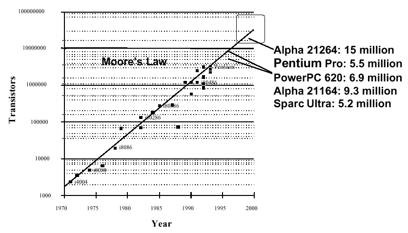
Figure 1.6. Exponential increase in processor capacity as
a function of time since the early 1970s (Moore's Law),
adapted from [Maf01].
The increase in processor capacity has made it possible to increase the speed of processor circuitry, particularly for arithmetic logic operations. For example, the chip area (also called real estate) required by an N-digit multiplier circuit varies approximately as N2. Thus, if the processor area doubles every 1.5 years, then the speed increase of a multiplier possible with such technology could increase by a factor of 21/2 = 1.414 times every 1.5 years. We see this reflected in the performance increases shown in the following section.
1.3.3. Processor Performance
In order to measure processor performance, we use the units of SPEC benchmarks. The System Performance Evaluation Cooperative (SPEC) benchmark suite was created in 1989 to rpovide a consistent set of realistic benchmarks for evaluating CPU performance. The SPEC95 set of benchmarks includes games, a hardware simulator, file compression and decompression, applications such as quantum physics simulations, fluid dynamics problem solutions, and so forth. In Figure 1.7, we show the increase in processor performance as a function of the SPEC92 benchmark suite, which is listed in Gee et al.'s analysis of cache performance. (Cache is a type of fast memory that we will discuss later in this course.)
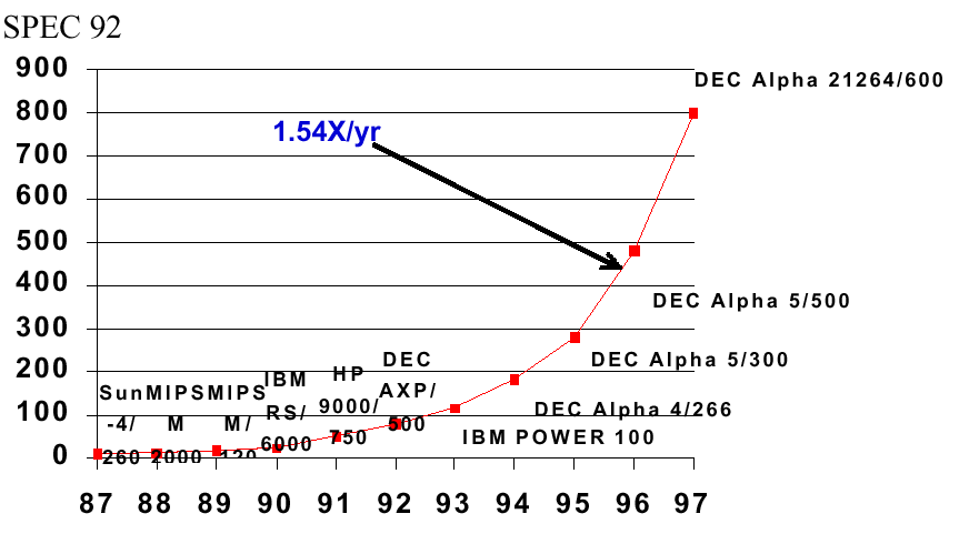
Figure 1.7. Exponential increase in processor performance as
a function of time since the early 1970s,
adapted from [Maf01].
The increase in processor performance has made it possible to port real-world applications to the PC platforms (e.g., Pentium and Apple G4 PC architectures). In the preceding section, we said that a multiplier's speed could increase 1.414 times every 1.5 years. So why does the curve in Figure 1.7 show an increase in processor capacity of 1.54 times per year? Consider that, although the previously-mentioned N-digit multiplier requires area proportional to N2, there exist many operations that only need area proportional to N. The mix of these applications and the operations that they use is highly dependent on the applications being run on the computer. Hence, the use of a benchmark suite such as SPEC92 or SPEC95 (discussed in the textbook), to provide a consistent mix of operations across all platforms and test scenarios.
1.3.4. Physical Limits on Computer Capacity and Performance
In the preceding presentation of hardware technology trends, there is danger in assuming that these trends will continue forever. In fact, there are physical limits to computer chip size and speed, which we will discuss briefly in this section.
Currently, computer chips are made by a process called lithography, in which the chip design is laid out with the aid of a computer, then printed onto a master template having multiple layers. This template is called a lithograph, after the printing process of that name. Masks are made from the lithograph master and are used to allow (or mask) the penetration of high-energy radiation into the semiconductor materials that comprise the chip. This irradiation process supports chemical removal of materials that comprise the partially completed semiconductor circuit, which is called etching.
Present lithography processes support 0.18 micron resolution (size of the smallest feature that can be produced on the chip). Making these dimensions smaller, to pack more transistors on the chip, requires the lithography process to use wavelengths of electromagnetic energy that are much smaller than visible light. Thus, it is foreseen that litho processes will progress through the ultraviolet range, down into X-ray and gamma-ray lithography, as technology is developed.
However, the limiting constraint is not how small we can make features on a circuit board. Rather, the hard limit involved in using computer circuits that we have today is dictated by the size of an atom. For example, when the thickness of an insulating strip between two conductors on a circuit board becomes less than approximately 1.2 atomic diameters, then there is significant interference or cross-talk between conductors or channels in an information-carrying structure called a bus. Given today's resolution of 0.18 microns, and the limiting atomic dimension of approximately 1nm (0.001), we only have approximately a factor of 200, or less than 2.5 orders of magnitude increase in resolution left in the current technology. That translates to a capacity increase of approximately 2502 = 62,500, which is not a comforting margin of safety. If Moore's Law continues to hold, then we the number of capacity-doubling periods is given by
Np = log2(62,500) < 16 ,
which translates to less than 16(1.5) = 24 years left in the technology cycle. Dr. Moore's current estimate is that we will run out of capacity in 2017, others say as late as 2025. What is certain is, that within your professional lifetime as computer scientists, there will be a radical shift from current circuit technology to something different - a technology that will support much faster, more highly parallel computing. Perhaps quantum computing will emerge as the dominant technology. Others say that biological computers based on DNA or protein technology will come to the rescue. IBM has recently announced the possibility of building circuits from carbon nanotubes, which presently have a width of approximately 10 atomic diameters. Whatever will happen, the paradigm shift will have profound technological and economic effects on the computer industry.
There is an interesting article about future technology trends at CNN's Web site that discusses Extreme Ultraviolet Photolithography for chip making - a useful summary of things that might occur.
If you want to read more about physical limits on computing, visit Dr. Frank's Web page about physical limits on computation. He has taught a course in this area, and the references listed therein make for interesting reading.
We next present overview of the types of computer architectures that have been developed with the technologies that have evolved since the dawn of useable computers during WWII.
1.3.5. Types of Architectures
There are three principal ways to connect components in a computer, called the von Neumann, bus, and multiprocessor architectures. We summarize each of these, as follows.
1.3.5.1. von Neumann Architecture. John von Neumann elucidated the first practical stored-program computer architecture (scheme for connecting computer components) in the mid-1940s. It is comprised of the five classical components (input, output, processor, memory, and datapath). The processor is divided into an arithmetic logic unit (ALU) and control unit, a method of organization that persists to the present. Within the processor, the ALU datapath mediates data transfer for computation. The registers are fast memory modules from/to which data can be read/written to support streaming computation, as shown in Figure 1.8. Within the ALU, an accumulator supports efficient addition or incrementation of values corresponding to variables such as loop indices.
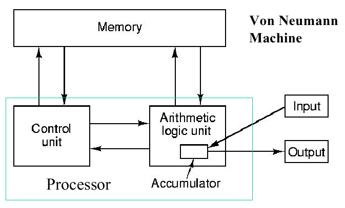
Figure 1.8. Schematic diagram of von Neumann architecture,
adapted from [Maf01].
The von Neumann architecture has a significant disadvantage - its speed is dependent on the bandiwdht or throughput of the datapath between the processor and memory. This is called the von Neumann bottleneck.
1.3.5.2. Bus Architecture. There are many animals (e.g., cat or dog) whose internal organs are hung from a backbone that conveniently happens to be horizontal. Bus-based computers are structured like that - processors and memory are connected to a backbone bus that acts as a "superhighway" for data or instructions to move between processors and memory. In practice, the bus architecture has the same components as the von Neumann architecture, but they are arranged along a bus, as shown in Figure 1.9.
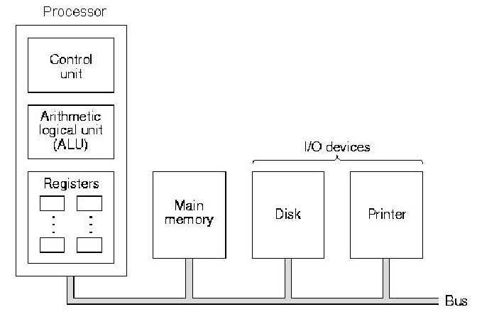
Figure 1.9. Schematic diagram of a bus architecture,
adapted from [Maf01].
In principle, the bus computer solves the von Neumann bottleneck problem by using a fast bus. In practice, the bus is rarely fast enough to support I/O for the common case (90 percent of practical applications), and bus throughput can be significantly reduced under large amounts of data. Figure 1.10 shows the layout of components in a modern PC, which is a useful example of a bus architecture.

Figure 1.10. Schematic diagram of PC bus architecture,
adapted from [Maf01].
In Figure 1.10, note that there are multiple buses - the PCI bus mediates large-scale data transfer between external components, as does the ISA bus. The SCSI bus is used to daisy chain peripherals such as disk drives, scanner, etc. The von Neumann bottleneck is partially overcome in practice by using a very fast bus, called the memory bus, to connect the CPU, memory, and the PCI bus.
Unfortunately, there are physical limits on how many components can be packed in a given space in a von Neumann machine (or any other computer, for that matter). Bus bandwidth limits the sequential computation model inherent in the von Neumann architecture to speeds that are not feasible for compute-intensive scientific applications. As a result, multiprocessor architectures were developed to address such problems, as discussed in the following section.
1.3.5.3. Multiprocessor or Parallel Architecture. Recall the old saying, "Many hands make less work." In computers, the use of many processors together reduces the amount of time required to perform the work of solving a given problem. Due to I/O and routing overhead, this efficiency is sublinear in the number of processors. That is, if W(N) [or T(N)] denotes the work [or time to perform the work] associated with N processors, then the following relationships hold in practice:
W(N) < N · W(1)
and
T(N) > T(1)/N .
The first equation means that the work performed by N processors working on a task, where each processor performs work W(1) [the work of one processor in a sequential computation paradigm], will be slightly less than N times W(1). Note that we use "<" instead of "=" because of the overhead required to (1) divide up the problem, (2) assign the parts of the problem to N processors, (3) collect the partial results from the N processors, and (4) combine the partial results to achieve a whole, coherent result.
The second equation means essentially the same thing as the first equation, but the work is replaced by time. Here, we are saying that if one processor takes time T(1) to solve a problem, then that same problem solved on an N-processor architecture will take time slightly greater than T(1)/N, assuming all the processors work together at the same time. As in the preceding paragraph, this discrepancy is due to the previously-described overhead.
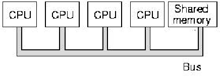
Figure 1.11. Schematic diagram of multiprocessor architecture, where
each CPU shares a memory module that is connected to a common bus -
adapted from [Maf01].
Figure 1.11 illustrates schematically a simple multiprocessor architecture with four CPUs, which share a memory module that is connected to the CPUs via a common bus. This is a simple architecture that is useful for solving selected types of compute-intensive problems. However, if you try to solve data-intensive problems on such an architecture, you encounter the von Neumann bottleneck trying to read and write the large amount of data from and to the shared memory.
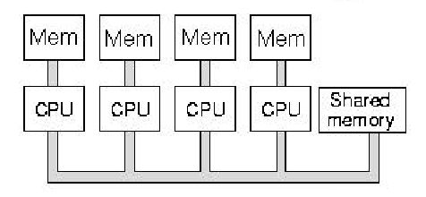
Figure 1.12. Schematic diagram of multiprocessor architecture with
shared memory, where each CPU also has its own fast, local memory -
adapted from [Maf01].
To help solve the problem of bus contention inherent in shared-memory multiprocessors, computer scientists developed the mixed model of parallel processing, in which the CPUs have small, very fast local memories that communicate with the CPU via a very fast, short bus. Because the bus is short, there are fewer impedance problems and the bus bandwidth can be increased. This migrates the von Neumann bottleneck closer to the CPU, and alleviates some of the demands on shared memory. Local memory architectures are useful for problems that have data locality, where (1) each CPU can solve part of a problem with part of the problem's data, and (2) there is little need for data interchange between processors.
A special type of multiprocessor is called a distributed processor, in which the individual CPUs (called compute servers) are connected to storage servers by a network. You can make the multiprocessor diagrammed schematically in Figure 1.12 into a distributed computer by replacing with a network the bus that connects the CPUs to each other and to the shared memory.
Having taken a high-level tour through computer technology trends, we next examine the low-level technology that makes these machines work, namely, digital logic.
1.4. Digital Logic Design
Reading Assignments and Exercises
Digital logic is hardware that implements the functions of Boolean algebra, which are or, and, not, as well as combinations of these functions. Boolean algebra operations are extensively employed in computing, and form the basis for the vast majority of arithmetic operations, as we shall see later in this course.
We begin this section by discussing the operands and operations that comprise Boolean algebra, then show how these logical operations are implemented in simple digital devices.
1.4.1. Theory of Logical Operations
The kind of logic that we use in computing is generally called formal logic, which is one of the three bases of mathematics. (The other two bases are measurement theory and algebraic manipulation.) The type of formal logic that we will use in this course is called Boolean logic or Boolean algebra (the terms are interchangeable). There are other types of formal logics, such as interval logic (often called fuzzy logic), but we will not consider them in this course.
Definition. An algebra is a tuple A = (F,O) that contains a set of values F and a set of operations O on those values.
Example. The algebra of real numbers contains operations such as addition, multiplication, and division, with operands selected from the real numbers R.
Definition. Boolean algebra B = ({0,1}, O) contains a set of operations O called logical-or, logical-and, logical-not, etc., that operate upon numbers in the set {0,1} (i.e., operate on zero(es) or one(s)).
Example: logical-not - The not function inverts the value of its input. Thus, 0 = not(1) and 1 = not(0). Because the not function has only one input, it is called a unary operation.
Example: logical-and - The and function takes the minimum of its two inputs. Thus, 0 = and(0,0) = and(0,1) = and(1,0). However, 1 = and(1,1). Because the and function has two inputs, it is called a binary operation. (This use of the word "binary" is similar to calling the set {0,1} the "binary numbers", because there are only two numbers in the set.)
Example: logical-or - The or function takes the maximum of its two inputs. Thus, 0 = or(0,0), with 1 = or(0,1) = or(1,0) = or(1,1).
It is important to note that all logical operations can be constructed from not and and. In your discrete mathematics course (COT3100 at UF/CISE), you will see (or have seen) how to do this. For now, it is useful to accept this assertion and continue on.
We next consider how digital logic is represented in term of truth tables and graphic symbols used in circuit diagrams. In Section 1.4.3, we will discuss how digital logic can be implemented in hardware.
1.4.2. Representations of Digital Logic
When we are working with digital logic, it is easy to describe the functionality of a logic device in terms of a truth table.
Definition. A truth table is a tabular representation of a logical operation that completely defines the operation.
Observation. A logical operation with N inputs will have 2N entries in its truth table. If an operation has many inputs, then its truth table can be represented compactly by listing only those entries that have nonzero output.
There are also a variety of graphic symbols that are used with digital logic functions. In Figure 1.13, we show the symbols for the and as well as or gates, with their truth table representations. If we represented these truth tables compactly, then the and operation would have only one row in its truth table, namely, [1 1 1].
Self-Exercise. How many rows are there in the compact representation of the or operation's truth table, and what are these rows?
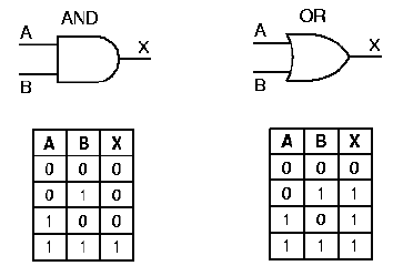
Figure 1.13. Graphic symbols and truth tables for the logic
gates that implement and as well as or operations,
adapted from [Maf01].
The not gate is represented graphically as shown in Figure 1.14a. By appending a circle to the output of a gate symbol, we can represent the effect of putting a not gate after the gate represented by the symbol. For example, the output of the and gate is inverted by the not gate to form the nand gate, as shown in Figure 1.14b. A similar situation is shown for the nor gate in Figure 1.14c. Note that the truth table for the nand operation has three nonzero entries, whereas the truth table for the and operation had only one nonzero entry. A symmetric condition exists for the nor operation.
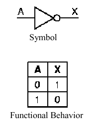
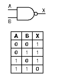
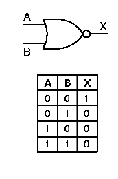
Figure 1.14. Graphic
symbols and truth tables for negative logic gates that implement (a)
not, (b) nand, (c) nor operations - adapted from
[Maf01].
In the next section, we discuss how these basic gates are implemented in electronic circuits.
1.4.3. Circuit Implementation of Digital Logic
In 1947, scientists at Bell Laboratories developed the transistor, which is a circuit element whose conductivity varies with applied voltage. The advantage of the transistor is that a relatively small input current can be used to control a much larger power-supply current. The general concept involved in the operation of the transistor is similar to that of the vacuum tube (recall our discussion of first-generation computers), but requires much less power and space. Also, the transistor can change state much more quickly than a vacuum tube - as sometimes said in electrical engineering, the transistor has a higher switching frequency.
1.4.3.1. Simple Model of A Transistor NOT Gate. Figure 1.15 shows a diagram of a transistor that implements negative logic. Note that the collector supply voltage Vcc is positive, and the current from this power source flows through a current limiting resistor, whose symbol is the jagged line below Vcc. The resistor is designed to prevent damage to the transistor junction, which is delicate. (This junction is comprised of several semiconducting materials deposited on a small wafer of silicon or germanium called substrate. As we discussed in Section 1.3, the dimensions of features etched into the substrate are presently on the order of 0.2 micron, so it doesn't take much excess current to cause electrical arcing across these features, which renders the transistor useless.)
A control voltage (shown in Figure 1.15 as the input signal A) is applied to the base of the transistor. If A = 0, the conductivity of the transistor is low, and the current from the collector is not grounded at the emitter. This causes a voltage difference to be present between the emitter (at ground) and the collector (at Vcc). Symmetrically, when A = 1 (i.e., a voltage significantly higher than zero), then the conductivity of the transistor is enhanced, and Vcc is grounded. This produces little or no voltage drop across the collector-emitter junction, and the output at the collector is effectively zero. When the output of the transistor is taken from the collector (as shown in Figure 1.15), these two conditions cause a not operation to be implemented.
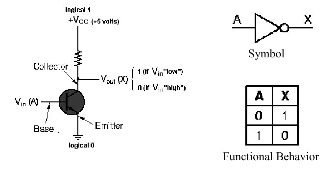
Figure 1.15. Transistor implementation of a NOT gate,
adapted from [Maf01].
1.4.3.2. NAND Gate Circuit. The nand gate is implemented using the operating principle of the not circuit shown in Figure 15. As shown in Figure 1.16, if both transistors have a high input (A = 1 and B = 1), then both transistors conduct, and Vcc is grounded. This produces little or no voltage drop from the voltage supply to ground, and near-zero voltage (logical zero value) occurs at the gate's output. This implements the entry for zero output in the nand gate's truth table, shown again in Figure 1.16 for purposes of verification.
If either (or both) input(s) of the nand circuit shown in Figure 1.16 is (are) low, then the two transistors taken together do not form a conducting path, and there is a significant voltage drop (logical one) at the gate output. This implements the nonzero entries of the nand gate's truth table.
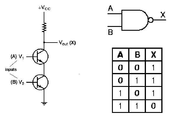
Figure 1.16. Transistor implementation of a NAND gate,
adapted from [Maf01].
1.4.3.3. NOR Gate Circuit. The nor gate is implemented using the operating principle of the not circuit shown in Figure 15. As shown in Figure 17, if both transistors have a low input (A = 0 and B = 0), then both transistors do not conduct, and Vcc cannot be grounded. This produces a significant voltage drop from the voltage supply to ground, and a logical one value occurs at the gate's output. This implements the sole entry for unitary output in the nor gate's truth table, shown again in Figure 17 for purposes of verification.
Conversely, if either (or both) input(s) of the nand circuit shown in Figure 1.16 is (are) high, then either (both) transistor(s) form a conducting path that grounds Vcc, yielding no significant voltage drop (logical zero) at the gate output. This implements the zero entries of the nor gate's truth table.
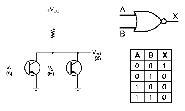
Figure 1.17. Transistor implementation of a NOR gate,
adapted from [Maf01].
Integrated circuits often contain multiple gates in one in-line package. For example, the layout of a quad nand gate IC is shown in Figure 1.18. Note that the notch in the circuit packaging material, shown on the left-hand side of the IC, helps orient the IC user to the pin ordering scheme. Each nand gate input and output pin is unique, with a pin for the common supply voltage Vcc, and another pin for common ground.
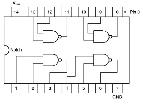
Figure 1.18. Example of quad nand gate integrated circuit
pin-out diagram, adapted from [Maf01].
We next examine how the laws of Boolean algebra can be used to generate designs for more complicated logic circuits.
1.4.4. More Complex Logic Circuits
In this section, we present several examples of how complex logic circuits can be designed from equations that represent the circuit's functionality, or from truth tables.
1.4.4.1. Laws of Boolean Algebra. Each type of formal logic has rules for manipulating operations and operands. In Boolean algebra, the following rules hold:
Assumption. Let B = {0,1}, with
p,q,r  B and
x,y,z
  R. This
assumption will hold for the subsequent discussion.
Identity. In arithmetic with real numbers, x · 1 = x and x + 0 = x. In logic, the analogous statements are
p and 1  p,
and p or 0
  p .
p .
Domination. In arithmetic with real numbers, x · 0 = 0. The logical analogue is
p and 0  0 .
0 .
Symmetrically, p or 1  1 .
1 .
Idempotency. This property can be used to simplify and or or operations, i.e.,
p or p  p
p
p and p  p .
p .
Double Negation. In arithmetic, -(-x) = x. In logic,
not(not(p))  p.
p.
Commutativity. In arithmetic, addition and multiplication are commutative, i.e., x + y = y + x and x · y = y · x. In logic, we have analogous formulations:
p or q  q or p
p and q  q and p .
Associativity. In arithmetic, addition and multiplication are associative, i.e., (x + y)+ z = x + (y + z) and (x · y) · z = x · (y · z). In logic, we have the analogous formulations:
(p or q) or r  p or (q or r)
(p and q) and r  p and (q and r) .
Distributivity. In arithmetic, multiplication distributes over addition. In logic, we have a similar situation:
p and (q or r)  (p and q) or (p and r)
p or (q and r)  (p or q) and (p or r) .
DeMorgan's Laws. Manipulation of logical statements is greatly aided by DeMorgan's laws, which describe a property that resembles distributivity:
not(p or q)  not(p) and not(q)
not(p and q)  not(p) or not(q) .
Self-Exercise. Construct truth tables for (a) distributive and (b) DeMorgan's Laws, listed above.
1.4.4.2. Circuit Equivalence. Using the preceding equivalences, especially DeMorgan's laws, it is possible to transform one circuit form (e.g., nor logic) into another form (e.g., nand logic). Here, nor logic uses nor gates, and symmetrically for nand logic.
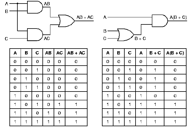
Figure 1.19. Example of quad nand gate integrated circuit
pin-out diagram, adapted from [Maf01].
For example, Figure 1.19 shows a circuit that outputs a one when inputs A and C are both one, or when A and B are both one, and outputs a zero otherwise. Note that the left-hand circuit has the same truth table as the right-hand circuit. Also note that the circuit equation for the left-hand circuit (AC + AB) can be rewritten using the distributive law (from Section 1.4.4.1) to yield A(C+B), which is the equation for the right-hand circuit. Here, the minterm AC means (A and C), and the minterm C + B means (C or B).
Logic transformations are primarily used for circuit minimization. For example, Note that the right-hand circuit in Figure 1.19 has only two gates, while the left-hand circuit uses three gates. This is because the expression AC + AB requires three operations (two and, one or), while the expression A(C + B) requires two operations (one and, one or).
1.4.4.3. Majority-Vote Circuit. Given N inputs a1, a2, ..., aN, the majority vote function outputs a one when N/2 or more of the inputs are ones, and zero otherwise. (If N is odd, then N/2 is rounded up to the nearest integer.) Figure 1.20 illustrates a logic circuit that implements the majority vote function for three inputs. Observe that the inputs A, B, and C and their negations (represented by a bar above each variable) are present in buses (vertical lines), then are combined to form the four minterms listed in the equation for M. Including the not gates used for negation, eight gates are required to implement this circuit. Note, however, that the and gates each have three inputs (corresponding to the three variables in each minterm) and the or gate that produces the circuit output has four inputs (corresponding to the four minterms of the equation for M).
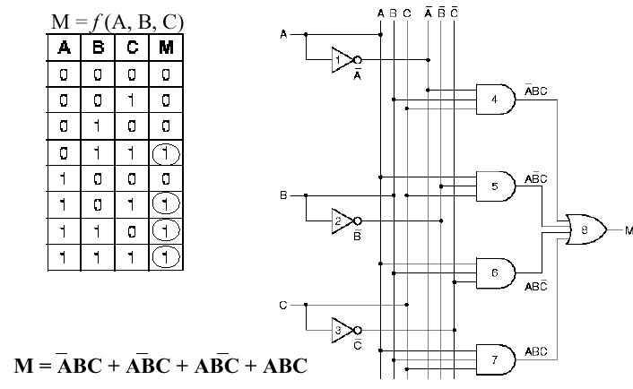
Figure 1.20. Example of Majority Vote Circuit, its truth table,
and the governing equation, adapted from [Maf01].
Self-Exercise. How many minterms would there be in the equation for the majority-vote circuit with four inputs? five inputs? N inputs?
1.4.5. Comparators and Combinatorial Logic
Combinatorial logic circuits include multiplexers, demultiplexers, encoders, decoders, and comparators. A combinatorial circuit has many inputs and one (or, sometimes, more than one) output. The output(s) of a combinatorial circuit are uniquely determined by the inputs. Combinatorial circuits have no memory elements. We will begin our discussion of combinatorial circuits with the simple example of a comparator, then progress to the multiplexer and decoder.
1.4.5.1. Comparator. It is often useful to determine whether or not two operands are equal, which is called comparison. A digital logic circuit that determines whether or not two four-bit operands A = (A0,A1,A2,A3) and B = (B0,B1,B2,B3) are equal is shown in Figure 1.20. The algorithm that the circuit implements is based on the concept of an exclusive-or operation (also called an xor operation), which is instantiated in an xor gate.
The xor function resembles the inclusive or, except that when both inputs are high, the xor output is zero, as shown in the following truth tables:
                 A   B   X                 A   B   X
             -+---------------         -+---------------
          xor |  0   0   0          or  |  0   0   0
              |  0   1   1              |  0   1   1
              |  1   0   1              |  1   0   1
              |  1   1   0              |  1   1   1
After the xor operation is applied to each bit of A and B (we call this bitwise processing), the xor outputs are operated on by a quad-input nor gate. Thus, if any of the bits are different, the or part of the nor gate will return a one, and the not part of the nor gate will return a zero. If A0 = B0 and A1 = B1 and A2 = B2 and A3 = B3, then the nor gate will applu the or operation to the outputs of the xor gates (which will all be one) to yield a one, which will be inverted at the output of the nor gate to yield a zero.
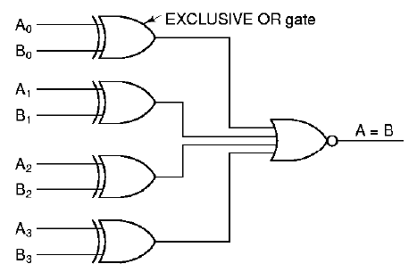
Figure 1.21. Example of Comparator Circuit, adapted from [Maf01].
1.4.5.2. Multiplexer. A multiplexer has n control signals and 2n inputs (sometimes called data lines). The purpose of a multiplexer is to use the control signals to decide which of the inputs will be routed to the multiplexer's output. Thus, the multiplexer is a type of switching device that chooses its output from among its inputs, based on control signals.
For example, Figure 1.22 illustrates a multiplexer with n = 2 control lines (A, B) and 2n inputs (D0 through D3). Note that inverters (not gates) provide the complement of A and B for constructing the minterms of the circuit's governing equation.
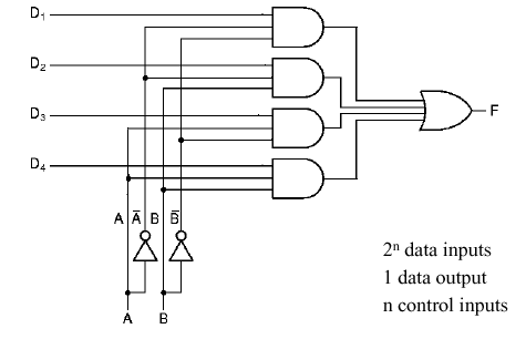
Figure 1.22. Example of Multiplexer Circuit, adapted from [Maf01].
Self-Exercise. Write the governing equation of the multiplexer shown in Figure 1.22. How does this compare with the governing equation of the majority-vote circuit shown in Figure 1.20? In what detailed ways are these circuits different?
1.4.5.3. Decoder. A decoder can be loosely thought of as a kind of reverse multiplexer, without the control lines. A decoder has n inputs, and 2n outputs. The input indexes the output - for example, if the input is 000, then the output D0 will be high. If the input is 001, (or 010) then the output D1 (resp. D2) will be high, and so forth.
For example, Figure 1.23 illustrates a decoder with n = 3 inputs (A, B, C) and 2n = 8 outputs (D0 through D7). As in the multiplexer circuit, inverters provide the input complements for constructing the minterms of the circuit's governing equation.
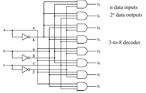
Figure 1.23. Example of Decoder Circuit, adapted from [Maf01].
Self-Exercise. Write the governing equation of the decoder shown in Figure 1.23. How does this compare with the governing equation of the multiplexer shown in Figure 1.22? In what detailed ways are these circuits different? (Hint: Think about minterms, complementation, and DeMorgan's laws.)
Thus, decoders can be used to select one object from a large number of indexed objects, given a Boolean representation of the index of that object at the decoder's input. For example, if the decoder outputs each control a relay that switches a voltage through a different resistor value, then it is possible to construct an n-to-2n decoder that converts an n-bit input signal into an analog voltage ranging from zero to 2n units. However, the circuitry for large n can become prohibitive, so this technique is of pedagogic interest only.
1.4.6. Programmable Logic Arrays
It is readily seen that circuits such as those shown in Section 1.4.5 can become prohibitively complex, large, and power-consumptive if implemented on a circuit board with many chips containing various types of logic gates. Thus, it is reasonable to ask how we might put a complex digital circuit on a chip. There are two ways to do this. First, the circuit can be custom-fabricated, which is very expensive, especially for small quantities. Second, one can use programmable logic, which provides many different types of gates on a chip, with a programmable network of interconnects between the gates. Programmable logic has widespread software support, so it is relatively easy (using modern design tools) to design a circuit, reduce it to a logic schematic (diagram of connectivity and parameters of logic elements in a circuit), then use a computer to program a special logic device called a PLA (programmable logic array).
In Figure 1.24, we illustrate a simple PLA circuit. This type of circuit is called two-level logic because there are two levels of processing (i.e., and gates at Level 1, or gates at Level 2).
Self-Exercise. What are the two levels of processing in the circuits shown in Section 1.4.5?
In practice, programmable logic devices are made in a variety of gate configurations, connectivity networks, and gate densities. One of the more important types of PLAs is called FPGA, for Field Programmable Gate Array. FPGAs represent a new method of designing custom ICs. Unlike conventionals Gate Arrys, FPGAs can be designed and programmed by a computer user (e.g., a hardware designer), and represent an advanced stage of evolution from Programmable Logic Devices (PLD). FPGAs are advantageous because they have a much higher gate density than PLAs or PLDs, and offer greater flexibility. FPGAs are useful for rapid prototyping, especially of large or complex circuits. Designs can be described using (a) schematic layout tools, (b) synthesis from a hardware description language model, or (c) high-level language driven synthesis tools.
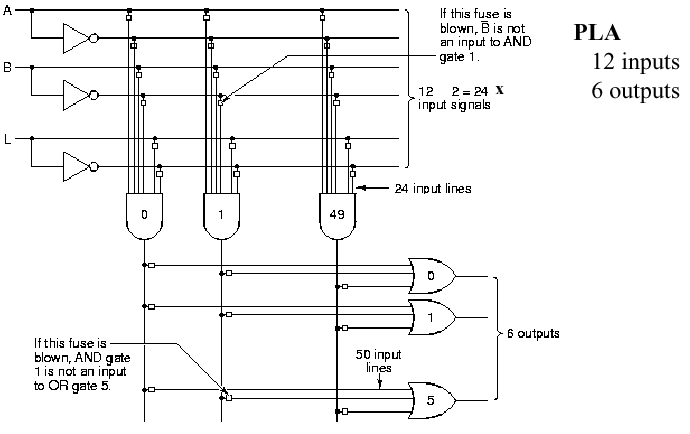
Figure
1.24. Example of programmable logic array, adapted from
[Maf01].
The circuit shown in Figure 1.24 is a fused-link circuit. To program this circuit, a software-driven programming device merely applies a large voltage to open-circuit (or "blow") each of the fuses (small boxes in Figure 1.24) that control access to a given input of a specific gate. For example, if the fuse at the junction of and gate #1 output and or gate #5 input is blown, then the and gate output cannot is not an input to that or gate.
There is a paper on the Web on Design of High Speed, Low Powered Dynamic Programmable Logic Arrays that is useful for advanced reading in this interesting topical area.
We next discuss clocked logic circuits.
1.4.7. Synchronous Logic
Thus far, we have considered only asynchronous logic circuits, in which the input pulses are allowed to propagate through the circuit at their own speed. This is acceptable for simple logic designs, but has the disadvantage that one needs to wait a short (usually somewhat indeterminate) time for the circuit output to stabilize. In time-critical applications where timing precision is required, the asynchronous approach to circuit design and implementation does not always produce useful results, due to indeterminacies in the output settling time.
To remedy this problem, synchronous logic circuits have been developed whose transition from one state to another is mediated by a clock pulse. (This can be thought of like people in a band playing in time to the conductor.) The vast majority of logic circuits use edge triggered clocking, which means that the state change in a circuit (e.g., from State Element 1 to State Element 2 in Figure 1.25a) occurs only when the clock pulse changes from a zero value to a one.

(a)
(b)
Figure 1.25.
State changes in logic circuits: (a) synchronous logic changes state
on the leading clock pulse (0-1 transition), and (b) asynchronous
logic does not require a clock to change state - adapted from
[Maf01].
To better understand synchronous logic, which is the dominant form in digital computing, we next examine how a clock works. We then discuss latches and storage circuits such as clocked latches and flip-flops.
1.4.7.1. Principles of the Clock. When we think of a digital clock, the image of a numerical timekeeping device comes to mind. However, in digital logic, a clock is really a very precise oscillator that changes its output from zero to one, then back to zero in a regular, predictable way.
For example, in Figure 1.26, a clock is comprised of an oscillator whose output is thresholded to form a train of rectangular pulses, called a square wave. The clock period is measured from one 0-1 transition to the next 0-1 transition. The addition of a delaying device after the clock output causes phase lag between the clock signals C1 and C2.
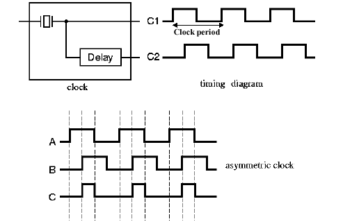
Figure
1.26. Example of clock output, with symmetric (A) and asymmetric
(B and C) clock pulses, adapted from [Maf01].
Within a clock cycle, there is the time a pulse is high (tH) and the time it is low (tL). If tH does not equal tL within a small measurement error, then we say that the clock pulse is asymmetric. This term also holds for a phase-shifted pulse, as shown in signal B of Figure 1.26.
If tH< tL within a small measurement error, then we say that the pulse duty cycle is less than one. This case is shown in Figure 1.26, for the clock signal labelled C. If tH > tL within a small measurement error, then we say that the pulse duty cycle is greater than one.
1.4.7.2. The SR Latch. Early in computing practice, it was desirable to store a bit in a small memory device. Since the only usable storage devices were relays (an electromechanical device) and delay lines that used the metal Mercury (chemical symbol Hg), it was decided to adapt asynchronous relay-based logic (very slow) to produce a storage element that could hold one bit.
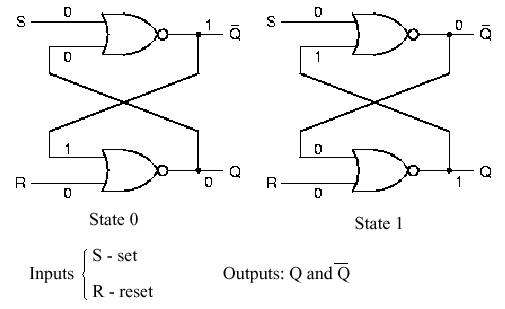
Figure
1.27. The two states of the SR latch, adapted from [Maf01].
Figure 1.27 shows a modern version of this concept, called the SR Latch, which is implemented in nor logic. (Using DeMorgan's Laws, it is possible to implement this in nand logic.) When the Set input is high and the Reset input is low, State 1 results, and conversely for State 0. Thus, the Set (Reset) puts a 1 (0) value at the output Q. It is not difficult to see that placing this circuit after an oscillator could product the clock pulses shown in Figure 1.26.
Self-Exercise. Derive the truth tables for State 0 and State 1 of the SR latch shown in Figure 1.27.
1.4.7.3. Clocked Latches. The problems with the asynchronous SR Latch shown in Figure 1.27 are (a) the S and R inputs can be energized at any time, and (b) settling of the circuit to yield its output value occurs immediately after the S or R signals are provided. This situation is remedied in the Clocked SR Latch of Figure 1.28, where two and gates are used in conjunction with a clock to drive the SR Latch of Figure 1.27.
The circuit works the same as the SR Latch, with the following important exceptions. First, if S or R are one, and the clock value is zero, then the output of the and gates is zero. If S or R equals one, and the clock is high, then the S,R values are passed to the input of the SR latch, but only while the clock is high. This gives the latch time tH to settle (see Section 1.4.7.1). If S or R are zero, then it doesn't matter what the value of the clock is - the inputs to the SR Latch remain zero.
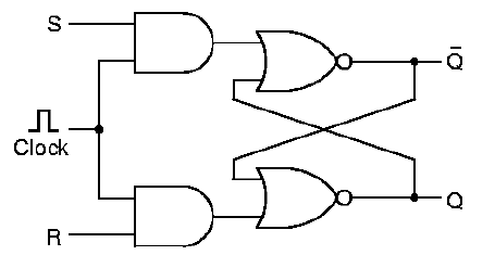
Figure
1.28. The Clocked SR Latch, adapted from [Maf01].
Self-Exercise. (1) Derive the truth table for the clocked input to the SR Latch in Figure 1.28, using the and gate logic, as shown. (2) Prove (using truth tables) how this could or could not be implemented in nor logic.
A problem with the clocked SR latch is that it has two inputs, and they have a forbidden configuration. Namely, one cannot apply both S = 1 and R = 1 to the circuit simultaneously - it won't know which state to enter! This problem is resolved with the Clocked D Latch, which is a minor variation on the clocked SR latch.
As shown in Figure 1.29, the D latch adds a not gate or inverter to the input of the clocked SR latch, so that its "S" and "R" inputs always have opposite values. In order to avoid confusion with the SR latch, the input is called D. The clock pulse is applied to the input, as it was with the SR latch.
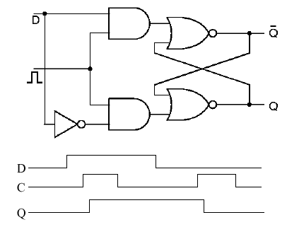
Figure
1.29. The Clocked D Latch, adapted from [Maf01].
As shown in Figure 1.29, the D latch has the following timing behavior (from the D,C,Q signals below the latch circuit). The D signal is the input (data), C is the clock, and Q is the output. When D goes high (0-1 transition), nothing happens to the latch until C goes high. (If D is low by the time C goes high, then the latch does not change state.)
If D is high and C goes high, then the latch changes state. There is a slight delay from the time C goes high to the time Q goes high, which is called the propagation delay (a function of the type of logic used, the semiconductor fabrication technique, wire lengths, etc.) When C goes low, whether or not D is high, the latch output (Q) stays high. This is the memory function of the SR latch that we discussed earlier. However, if D is low, then if C goes high (0-1 transition), Q goes low after the propagation delay occurs. Thus, the D latch only stores a unitary input (D = 1) for a time equal to the period of the clock. This can be verified by inspecting the timing diagram in Figure 1.29.
1.4.7.4. The D Flip-Flop. In order to make the D latch store a value throughout the high state of the clock, it is necessary to make a more complex circuit using the D latch, which we call a D flip-flop. The flip-flop is so named because it can be toggled back and forth between two states (Q = 0 and Q = 1) by varying D. The D flip-flop is comprised of two D latches and an inverter, as shown in Figure 1.30
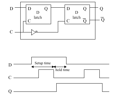
Figure
1.30. The D flip-flop with timing diagram, adapted from [Maf01].
Per Figure 1.30 the D flip-flop has the following timing behavior (determined from the D,C,Q signals below the latch circuit). When D goes high (0-1 transition), nothing happens to the latch until C goes high. (If D is low by the time C goes high, then the latch does not change state.) At the trailing edge of the clock pulse (1-0 transition), Q goes high if it was previously low. If Q was previously high, nothing happens to Q. When D goes low, nothing happens to Q until the clock pulse goes low. Then, after a propagation delay, Q goes low.
There are two critical time intervals associated with the D flip-flop. The setup time is the time required to keep D high, in order to wait for the trailing edge of the clock pulse. The hold time is the time required to hold D high after setup, to ensure that Q stays high.
Self-Exercise. (1) Derive the truth table for each of the four input states of the D flip-flop as shown in Figure 1.30. Hint: Input states are defined by the values of D and C (e.g., State 0: D = 0, C = 0->0; State 2: D = 0, C = 0 -> 1; etc.)
1.5. Computer Performance Assessment
Reading Assignments and Exercises
When we talk about computer performance, we need to consider the following issues:
Method of Performance Evaluation - By what measures will the performance be assessed? Will the assessment be local to a specific part of the computer hardware, or global (i.e., across all hardware and software modules)? What will the mix of instructions be?
Limitations of Evaluation - What are the shortcomings of each method or measure of performance assessment? From whence do these limitations arise, and why? What can be done to improve these limitations?
Metrics - What formal measures are to be used for performance evaluation? Speed? Time used in a computation? Memory space required?
Processor Performance Equation - How will the processor's performance be described mathematically? Does the equation portray actual parameters of practical interest, or does the computational model described by the equation not match the processing architecture under test?
Performance Evaluation Reports - What methods of analysis and presentation are used to evaluate data? Is the data normalized to a particular benchmark result or parameter? Is the normalization performed in a physically meaningful way?
Ahmdahl's Law - Whatever measurements are made, as one continues to enhance processor performance, the overall improvement achieves diminishing returns.
We examine each of thise issues, as follows.
1.5.1. Performance Evaluation
Computer performance evaluation is primarily based on throughput and response time. Throughput is how many bits of data are processed, or how many operations are performed, in a given interval of time. For example, we say that a processor has a throughput of N MB/s (megabytes per second). With respect to execution time of a program on a processor X, we say that
PerformanceX = 1 / Execution TimeX
and, for two processors X and Y,
Relative Performance = PerformanceX / PerformanceY
For example, in the preceding equation, if processor X is faster than processor Y, then Execution TimeX < Execution TimeY (all other things being equal), so Relative Performance < 1. This also implies increased throughput of X with respect to Y.
Key Concept. As a result, we want to improve performance by increasing performance, which means decreasing execution time. In practice, this can be done by (a) decreasing response time, or (b) adding more processors to a system (provided I/O is managed efficiently).
1.5.2. Measuring Performance
A program that is executing, or has been executed, has the following components:
Wall-Clock Time - how long it takes (typically, time in seconds) for your program to execute, from the time it is invoked to the time it completes. This time is measured with respect to a global time standard, so we name it according to a common object such as a wall clock. This is also called elapsed time.
CPU Time - comprised of user CPU time (time spent computing the program), and system CPU time (the time the operating system spends supporting the program).
I/O Time - time spend reading and writing data from/to memory.
Other Time - time spend running other programs, waiting for the operating system to be scheduled, etc.
We can measure a program's execution time using the
UNIX time command. For example, let's enter the UNIX
command time du at one's root directory (which can be
reached via the command cd. When I tried this on my
(large) directory tree, I got the following result:
0.21u 1.54s 0:24.49 7.1%
These four numbers have the following meaning:
User CPU Time = 0.21 seconds, the first number (
0.21u).System CPU Time = 1.54 seconds, the second number (
1.54s).Elapsed Time = 24.49 seconds, the third number (
0:24.49).CPU Activity as Percent of Elapsed Time = 7.1 percent, the fourth number (
7.1%).
Observe that percent CPU activity is computed as follows:
- Step 1. Add the User and System CPU Times to get Total
CPU Time (e.g., 1.75 sec = 0.21 sec + 1.54 sec).
Step 2. Divide the Total CPU Time by Elapsed Time (e.g., 0.071 = 1.75 sec / 24.49 sec).
Step 3. Multiply by 100 to get percent (e.g., 7.1% = 0.071 x 100 percent).
Other Time is computed as follows:
- Step 1. Add the User and System CPU Times to get Total
CPU Time (e.g., 1.75 sec = 0.21 sec + 1.54 sec).
Step 2. Subtract the Total CPU Time from Elapsed Time (e.g., Other Time = 22.74 sec = 24.49 sec - 1.75 sec).
Given a method of measuring time, and computation of different times (e.g., CPU, Other) from these measures of time, we can now discuss a simple model of computation for measuring CPU performance.
1.5.3. CPU Performance Equation
In order to measure CPU performance in a physically realistic way, we need a model of computation. In the simplest case, we start with the number of CPU cycles, defined as follows:
Ncyc = IC · CPI ,
where IC denotes the instruction count (number of instructions per program), and CPI denotes the average cycles per instruction.
Given the CPU cycle time tcyc or the clock rate BWclk, we can express the CPU time as:
tcpu = Ncyc · tcyc
or
tcpu = Ncyc · BWclk .
Patterson and Hennesey [Pat98] express this as

with units indicated for each variable.
If there are different types or classes of instructions in a given program, then the preceding equation for Ncyc is not an accurate estimate, because CPI can be affected by the instruction mix (nimber of each of type of instruction that occurs in the program). Thus, we use the following equation to more accurately determine the number of cycles incurred when a program is executed:
Ncyc =  CPIi · ICi ,
where we assume that there are n classes of instructions. The frequency distribution of instructions, which is comprised of (IC1, IC2, ..., ICn), is obtained by a technique called execution profiling, which is supported by a variety of commercial software tools. The number of cycles per instruction type is determined from analysis of a specific processor design, validated by performance measurement.
Example 1. To illustrate the practical utility of these measurements, let us assume that a program runs in 10 seconds on a processor with a 400 MHz clock rate. We want to build a new computer that can run the program in 6 seconds by increasing the clock frequency to X MHz. An unfortunate consequence is that the average CPI will be 1.2 times higher in the new processor. Here's how we set the problem up to determine the new clock rate X:

Solving the equation yields X = 800 MHz. Thus, we see that doubling the clock rate does not necessarily double the processor speed, because there are other variables (e.g., CPI or the instruction mix) that can be affected, as shown below.
Example 2. Now we will consider the effect of instruction mix. Assume that the following data are correct:
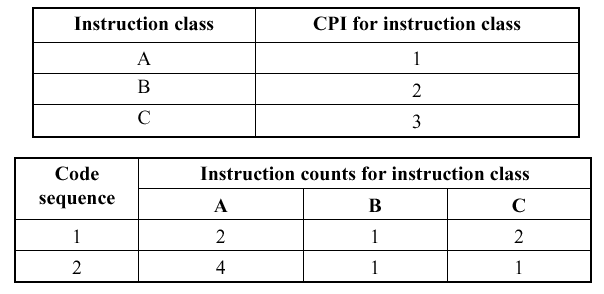
Q: Which code sequence will be faster - #1 or #2?
A: The sequence that incurs the least number of cycles is faster. Using the preceding equation for Ncyc we see that the number of cycles for code sequences 1 and 2 are given by:
Ncyc(Seq.1) = (2 · 1) + (1 · 2) + (2 · 3)
= 10 cycles
Ncyc(Seq.2) = (4 · 1) + (1 · 2) + (1 · 3)
= 9 cycles .
Thus, code sequence #2 is faster, because it requires 9 cycles, versus 10 cycles for code sequence #1.
1.5.4. Performance Evaluation
In an ideal situation, one has a suite of programs whose instruction mix is known exactly. By running each program on a processor to be analyzed, it is possible to determine CPI for each type of instruction. However, life is rarely ideal. Thus, we have the following types of benchmarking programs to measure and bound processor performance:
Synthetic Benchmarks are used to exactly measure specific characteristics of a processor (e.g., memory I/O performance, register-to-register I/O, speed of arithmetic functions, etc.) Because the benchmarking program is synthetic, one can put any combination of instructions into it, and the benchmark is not necessarily realistic.
Toy Benchmarks are simple but somewhat realistic programs that help the designer get a preliminary idea of a how a processor will behave under pseudo-realistic constraints. These might include tasks such as solving a simple matrix equation, performing a near-trivial image processing operation, etc.
Kernels are more involved programs that capture the functionality of a larger program. For example, one can use an operating system kernal to get an idea of the operating system performance on a given processor, provided that the kernal is executed significantly more in practice than the other programs in the operating system.
Real programs are used (a) to measure performance at many stages of processor design, (b) to estimate the processor's performance under realistic computing constraints and (c) in assessment of fielded systems.
In practice, realistic benchmarks include engineering or scientific applications, software development tools, transaction processing, and office applications such as large spreadsheets or formatting of word processing documents.
1.5.5. Performance Reporting
After one has measured the performance of a given processor, then one formulates a test report. In order to make our report accurate and meaningful to a hardware designer, we must have at least three elements in the report:
Hardware/Software Configuration tells the designer what benchmarking programs were run on the processor under test, and how the processor was set up (e.g., how much memory, what clock rate, compiler version, etc.)
Evaluation Process Conditions provide information about special constraints on the instruction mix that can influence the reproducibility of the performance measurement.
Performance Summary is typically expressed in terms of average rates. How these averages are computed is of practical interest.
For example, consider the following types of means:

Normalized results are not easily understood or accurately compared with the arithmetic mean, because the mean of ratios between two series of measurements is not the same as the ratio of the series means. Instead, normalized results should be combined with the geometric mean, which is independent of the data series used for normalization. This is because the ratio of two series' geometric means is the same as the mean of the ratios between the series.
That is, given two data series {Ai} and {Bi}, where i = 1..n, if the arithmetic mean is used, then
AM({Ai}) / AM({Bi})  AM({Ai / Bi})
whereas, with the geometric mean:
GM({Ai}) / GM({Bi}) = GM({Ai / Bi}) .
Here, the construct {Ai / Bi} means divide the i-th element of A by the i-th element of B. For example, if {Ai} = {2,4,6} and {Bi} = {2,2,3}, then {Ai / Bi} = {2/2, 4/2, 6/3} = {1,2,2}.
Example. The practical implications of this problem are illustrated in the following table:
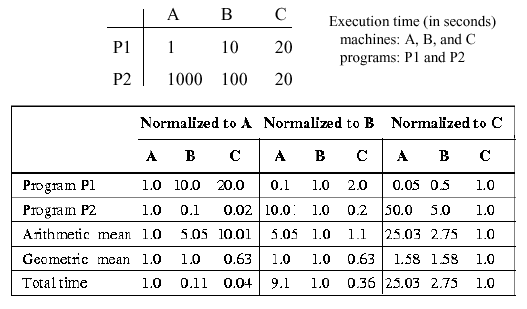
Here, "Normalized to A" means that the data for processors A, B, and C are divided by the data for A. In the first set, programs P1 and P2 are both normalized to A, hence, the arithmetic and geometric means for A are both 1.0 (the mean of 1.0 and 1.0 is 1.0). However, the arithmetic mean for B is 5.05 = (10.0 + 0.1)/2, while the geometric mean for B is 1.0, due to the previously-mentioned normalization property. Total execution time is likewise normalized in the first set, to the value for A, which is 1001 = 1000 + 1. Thus, the total time for B = 0.10989 = (100 + 10) / 1001, which is approximately 0.11.
Self-Exercise. (1) Derive all the entries in the preceding table. Be able to explain how each one was calculated. (A problem like this will likely be an exam question.)
1.5.6 Implications of Amdahl's Law
In the 1960s, Gene Amdahl derived an equation that expresses the diminishing returns that one obtains when trying to optimize a computer program. His equation has been adapted by Patterson and Hennesey, as follows:


This means that, the more you enhance the performance of a fraction f of a program or processor, the remaining (unenhanced) part (1 - f) gets progressively smaller. In order to keep the speedup S constant for each enhancement, you have to enhance performance of the remaining (1 - f) part to have a much greater speedup than S.
Example. Suppose a program takes 10 seconds to execute on processor P. After P's floating point (FP) unit is enhanced to be 5 times faster, then reinstalled in P, the effective speedup is graphed in Figure 1.31a. Here, the speedup is on the ordinate (vertical axis) and the fraction of the execution affected by the FP is on the abscissa. What is obvious is that in order to obtain a speedup of 2.0, the new FP has to be used approximately 0.65 (65 percent) of the time. In all but the most highly parallelized image or signal processing code, this is quite unlikely.
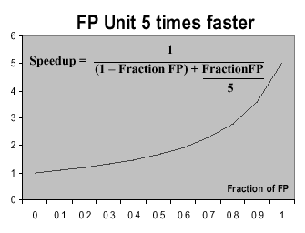
(a)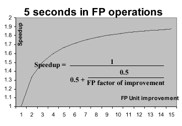
(b)
Figure 1.31. Amdahl's Law applied to processor performance enhancement,
adapted from [Maf01].
The situation worsens in Figure 1.31b. Here, we see that if the new FP unit affects only 1/2 of the program execution, then we will approach a speedup of 2.0 asymptotically, regardless of how much the FP unit's performance is improved. As in Figure 1.31a, the speedup is graphed on the ordinate, with the enhancement factor of the FP unit on the abscissa.
Amdahl's Law has important implications for practical computer design. Namely, if a portion of the CPU does not affect program execution very much, then there is little point in drastically enhancing its performance. As a result, we try to enhance the most frequent deficiencies first. This is called enhancing the common case and it works, for the reasons shown in the preceding example.
1.6. Performance Benchmarking
Reading Assignments and Exercises
As we discussed in Section 1.5, a benchmark is a program that is used to measure a computer system's performance in a more-or-less standardized way. We aspire to standard benchmarks because of the need for realism and reproducibility in performance testing. In the ideal situation, one can test a processor using a representative sample of real workload. In practice, one first characterizes the working set of programs statistically (e.g., number of operations of each type), then computes the time each program requires, based on the sum of the product CPIi · ICi over all instruction types.
We next overview different types of benchmarks and how they have been, or are, used in practice.
1.6.1. Linpack Benchmark
The Linpack benchmark is an old, well-established measure of CPU and ALU performance that measures the time required to solve a dense system of linear equations. In FORTRAN, the Linpack kernal resembles the following loop:
     DO 10 I = 1,N
       DY(i) = DY(i) + DA * DX(i)
 10  CONTINUE
Here, the "D" that precedes each variable denotes a double-precision operand. As a result, the Linpack benchmark challenges the ALU and control unit primarily. However, I/O is also challenged, due to the large data requirement associated with the vectors DX and DY.
Linpack has the following measures (also called metrics):
- Rpeak - peak system performance, in Gflops
- Nmax - matrix size that yields the highest
Rpeak
- N1/2 - matrix size that yields the 0.5 ·
Rpeak
- Rmax - Gflops achieved for the matrix of size Nmax
You can read more about the Linpack benchmark at http://www.top500.org/.
1.6.2. Intel's iCOMP Index 3.0
The iCOMP index is a geometric mean of relative performance measures (recall from Section 1.5 how geometric means work well with ratio-based metrics [also called ratiometric quantities]). The benchmark contains a mix of instructions that are assumed to characterize existing and emerging software. The iCOMP benchmark seems to be more relevant as the use of 3D graphics, multimedia, and Internet access increases.
iCOMP 3.0 has the following composition, with weighting indicated in percent:
- #1,2: Multimedia and Internet application (25%)
- #3: Two integer productivity applications (20% each)
- #4: 3D geometry and lighting calculations (20%)
- #5: Java application (10%)
- #6: Floating point: engineering, finance, and game applications (5%)
The preceding six benchmark results are combined as follows. Let the ratio BMi/Base_BMi denote the i-th benchmark performance, where BM denotes the benchmark run on a test processor, and Base_BM denotes the benchmark run on a baseline processor, in this case a Pentium II clocked at 350 MHz. The iCOMP benchmark is computed as:

where Pi denotes a weighted exponent that incorporates the 1/6 power (root) that comprises the outer operation of the geometric mean. Thus, the iCOMP index is a weighted geometric mean of application-specific performance ratios.
1.6.3. SPEC2000 Benchmarks
The System Performance Evaluation Corporation (SPEC) benchmarks are upgraded every 2-3 years, to account for the characteristics of software as program designs evolve. For example, longer run time, larger problems, and greater diversity of applications characterize newer software. The SPEC2000 benchmark has both baseline and optimized measures, comprised of the geometric mean of normalized execution times. The reference machine for SPEC2000 is a Sun Ultra5_10 (300 MHz SPARC architecture with 256MB of memory).
The current SPEC2000 suite is comprised of the following 12 integer and 14 floating point (FP) programs, which measure response time and throughput:
164.gzip(C, integer) - Compression175.vpr(C, integer) - FPGA circuit placement and routing176.gcc(C, integer) - C programming language compiler181.mcf(C, integer) - Combinatorial optimization186.crafty(C, integer) - Chess game197.parser(C, integer) - Word/language processing252.eon(C++, integer) - Computer visualization253.perlbmk(C, integer) - PERL programming language254.gap(C, integer ) - Group theory, interpreter255.vortex(C, integer) - Object-oriented database256.bzip2(C, integer ) - Another compression program300.twolf(C, integer ) - Place and route simulator168.wupwise(Fortran-77, FP) - Physics/quantum chromodynamics171.swim(Fortran-77, FP) - Shallow water circulation modelling172.mgrid(Fortran-77, FP) - Multigrid solver: 3D potential field173.applu(Fortran-77, FP) - Parabolic/elliptical PDEs177.mesa(C, FP) - 3D graphics library178.galgel(Fortran-90, FP) - Computational fluid dynamics179.art(C, FP) - Image recognition/neural networks183.equake(C, FP) - Seismic wave propagation simulation187.facerec(Fortran-90, FP) - Image processing: Face recognition188.ammp(C, FP) - Computational chemistry189.lucas(Fortran-90, FP) - Number theory/Primality testing191.mfa3d(Fortran-90, FP) - Finite-element crash simulation200.sixtrack(Fortran-77, FP) - High energy nuclear physics accelerator design301.apsi(Fortran-77, FP) - Meteorology: Pollutant distribution
SPEC2000 metrics derived from the integer benchmarks (#1-12, above) include:
SPECint2000: The geometric mean of 12 normalized ratios when each benchmark is compiled in highly optimized mode (also called aggressive optimization)SPECint_base2000: The geometric mean of 12 normalized ratios when compiled with normal optimization (also called conservative optimization)SPECint_rate2000: The geometric mean of 12 normalized throughput ratios when compiled with aggressive optimizationSPECint_rate_base2000: The geometric mean of 12 normalized throughput ratios when compiled with conservative optimization
There is also a similar set of floating point metrics.
The results of the SPEC2000 integer benchmarks are
shown in Figure 1.32, where the circle denotes the geometric mean, and
the spokes of the wheel whose rim is the circle denote individual
benchmarks keyed positionally to the diagram in the upper left-hand
corner. Note that the Mips processor with IRIX operating system performs
significantly worse than the mean on 181.mcf
(combinatorial optimization), and the three processors all perform
worse than the mean on 255.vortex (object-oriented
database) and 252.eon (computer visualization). Since
databases and visualization involve significant I/O, and visualization
involves significant amounts of graphics, it would be reasonable to
suggest that these areas need improvement in each of the three
processors tested.
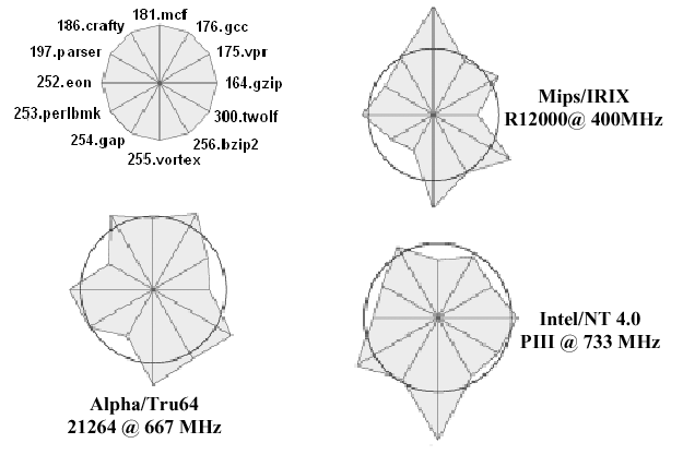
Figure 1.32. Test results for the SPEC2000 integer benchmarks
run on three processors, with key in the upper left hand corner,
after [Maf01].
The floating-point benchmarks shown in Figure 1.33
reveal similar discrepancies. For example, all processor perform
relatively poorly on the 179.art (neural net) benchmark,
which involves significant amounts of multiplication and division by
small magnitudes. It is interesting to note that, in both the integer
and floating point benchmark suites, the Intel Pentium III processor
appears to have the most uniform performance (largest number of
benchmark results closest to the mean). Since Intel is a contributor
to the SPEC benchmark suite, it is not surprising that their
processors could be designed to perform well on these established
benchmarks.
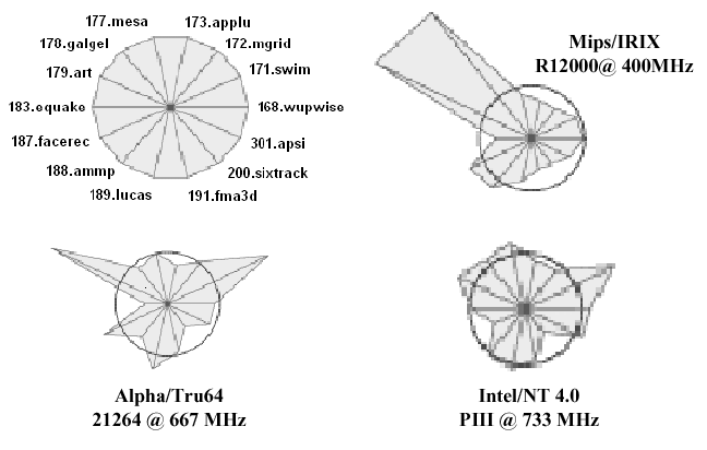
Figure
1.33. Test results for the SPEC2000 floating point benchmarks run
on three processors, with key in the upper left hand corner, after
[Maf01].
When the geometric means (of the SPEC95 integer and floating-point benchmarks) are respectively graphed as a function of clock rate, we have the results shown in Figures 1.34 and 1.35. Note that (a) SPEC95 is similar to SPEC2000, and (b) the performance of the Pentium Pro exceeds that of the Pentium due to microarchitecture improvements.
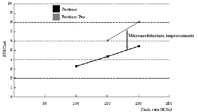
Figure
1.34. Graph of SPEC95 integer benchmark performance as a function of
processor clock rate in MHz,
adapted from [Maf01].
It can also be seen that the improvement in performance carries through to the floating point computations, as shown in Figure 1.35. However, the slope of the floating point benchmark curve for the Pentium is not as great as that for the integer benchmark. This could imply (depending on the statistical significance of the measurements) that the Pentium processor does not yield improvements as readily for floating point computations as it does for integer computations.
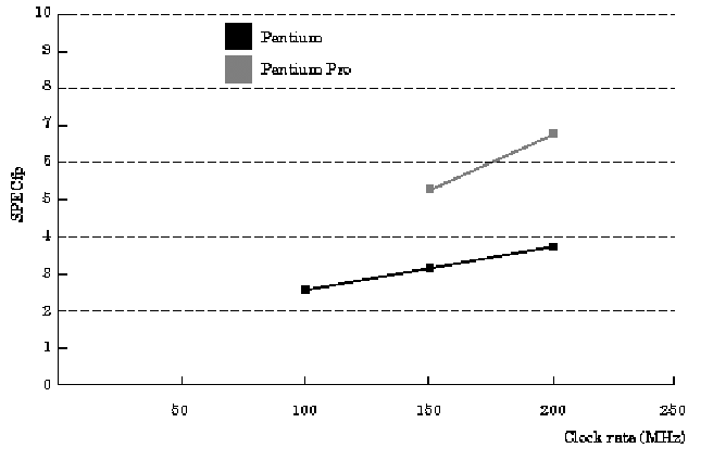
Figure 1.35. Graph of SPEC95 floating point benchmark
performance as a function of processor clock rate in MHz, adapted from
[Maf01].
1.6.4. MIPS Benchmark
The speed of a processor in millions of instructions per second (MIPS) can be estimated as:
MIPS = IC / (106 · tcpu) ,
where tcpu denotes CPU time. Unfortunately, due to different behavior characteristics of various processors (e.g., as shown in Figures 1.32 and 1.33) 1 MIPS on a given processor may not mean the same thing as 1 MIPS on another processor. In particular, MIPS is based heavily on instruction count (IC). This is like determining the winner of an auto race by who used fewer RPMs, or the winner of a marathon by who took fewer steps when running.
In practice, MIPS is especially misleading because floating point computations are done differently on different systems. For example, some computers do FP operations in software, while others use dedicated hardware units on- or off-chip. Also, the MIPS benchmark does not factor in the instruction mix, and thus compromises realistic characterization of workload.
The only situation where MIPS might be a useful benchmark is when the majority of variables have been fixed - for example, when comparing two processors from the same vendor that support the same ISA using the same compiler or the same benchmark suite. Apart from that, MIPS should be avoided as a measure of processor performance.
1.6.5. Fallacies and Pitfalls
When applying benchmarks to processors, one should avoid making the following mistakes:
Ignoring Amdahl's Law occurs when one tries to recursively optimize a processor, and puts much effort into the optimization process, only to achieve diminishing returns. Instead, one should optimize the common case first, then determine via a mathematical model such as Amdahl's Law whether or not further optimization is cost-effective.
Using MIPS as a performance metric is a common mistake, especially when one is in a hurry to portray a processor's performance in a favorable way. Instead, standard or well-established suites of benchmarks (such as the SPEC or iCOMP suite) should be applied to the processor, to highlight performance deficits in several categories.
Using the Arithmetic Mean of normalized CPU times is erroneous mathematically because the normalized CPU times are ratiometric quantities. As such, they cannot be combined into an ensemble statistic using the Arithmetic Mean. Instead, the Geometric Mean must be employed to combine ratiometric quantities.
Using "hardware-independent" measures such as code size defeats the purpose of hardware performance testing, namely, to highlight the specific advantages and deficits of a given processor. If the benchmark is hardware-independent, then it cannot produce information that is specific to a given architecture or processor. Instead, a suite of benchmarks such as SPEC or iCOMP should be used to identify hardware-specific performance deficits.
Assuming that synthetic benchmarks predict real performance is a major but common error. Recall from our discussion in Section 1.5, that synthetic benchmarks are programs devised by algorithm or hardware designers to measure specific types of performance on highly focused types of operation mixes. Because these benchmarks often bear little or no resemblance to real programs, they are of little use in characterizing a processor's performance in practical applications. Instead, a suite of benchmarks that is comprised of practical programs, such as SPEC or iCOMP, should be used.
Assuming that the geometric mean of CPU time ratios is proportional to the total execution time is erroneous for two reasons. First, the arithmetic mean, which is based on a sum, is proportional to total time. The geometric mean is based on a product and is thus not proportional to an accumulated (summed) total measure. Second, the CPU time is only part of the total execution time. Other factors that influence total time are I/O activity, wait time in a multiprocessor system, and network overhead in a parallel or distributed computing system.
In summary, performance measures are specific to a given program or suite of programs. CPU time is the only adequate measure of CPU performance - other metrics, such as I/O time or total time factor in effects that are not properly associated with the CPU (although they may be associated with a computer system). For a given ISA, performance increases result from (a) increases in clock rate, (b) improvements in processor architecture that reduce CPI, and (c) compiler enhancements that reduce IC (and, possibly, CPI) for a given type of instruction. The ideal benchmark is the workload that you plan to run on a given processor: all other assumptions about benchmarks can lead to unrealistic performance figures.